Related Voices

"India means Innovation" podcast episode: Innovation in the energy sector
Brandon Spencer, President, ABB Energy Industries shares insights on exciting challenges and opportunities in the energy transition with Snehil Gambhir, Partner Boston Consulting Group.

India Means Innovation
Nasscom, in collaboration with Boston Consulting Group (BCG), presents an exciting podcast series! Join industry leaders as they dive into the latest trends driving diverse industries, how the India's ER&D sector is innovating in India for the world.
India Means Innovation podcast episode: Innovation in the Automotive sector
Nasscom, in collaboration with BCG, presents the #IndiaMeansInnovation podcast series, exploring the trends driving transformation across industries. In this Episode: Snehil Gambhir, Partner and Director at BCG, along with Gilles Mabire, CTO, Automotive & Head of Software and Central Technologies, Continental AG discuss different aspects of the evolving automotive industry, and how the convergence of technology trends and consumer preferences are transforming this industry. They also discuss the emerging software-defined vehicle trend at length and how this opens new opportunities for incumbent players and tech companies in general.
#shemeansbusiness: Spotlightighting Nasscom Member Leaders
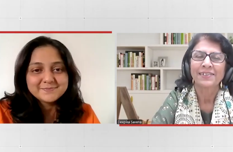
Listen to the inspiring journey of Deepika Saxena, President and CEO of NetEdge Computing Solutions Pvt. Ltd., and a Nasscom member. With a bold vision to transform the hiring process, Deepika harnessed the power of AI and automation to bridge the gap bet
#shemeansbusiness: Spotlighting Nasscom Member Leaders
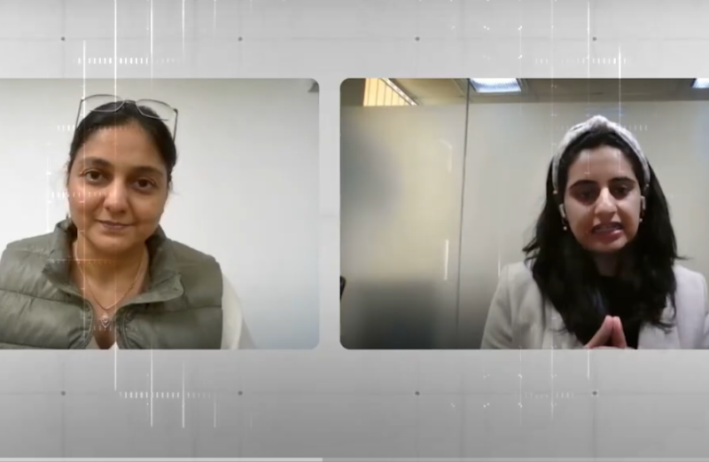
Vidushi Kapoor, CEO of Process Nine Technologies Pvt. Ltd. and Nasscom SME Council, shares her journey of driving innovation in language technology. With 15 years of expertise, she has made a mark in the Indian language industry, localization, and tech innovation.
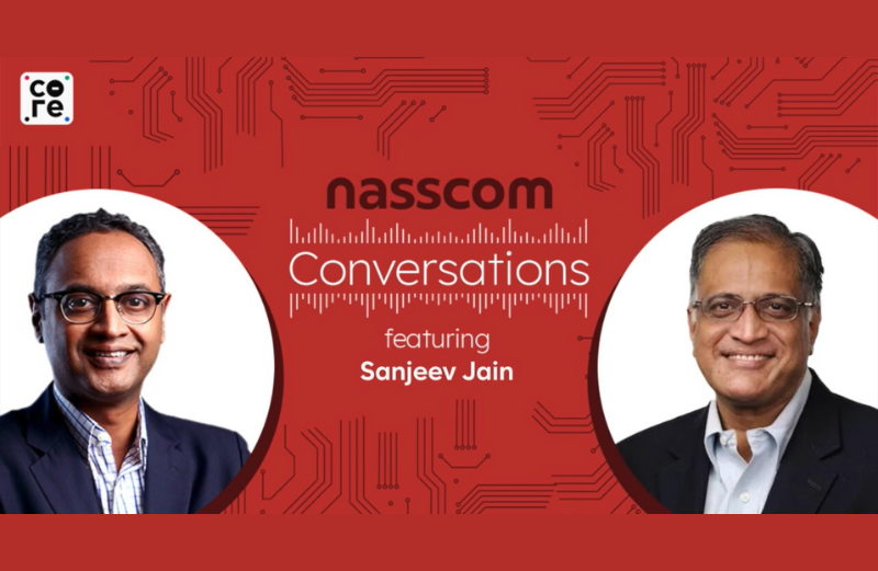
Building India’s AI Talent Ecosystem ft. Sanjeev Jain & Govind Ethiraj
From upskilling employees to driving innovation, AI is revolutionizing the way companies operate. In this episode, Sanjeev Jain, Member of the Executive Board and Chief Operating Officer at Wipro, explores India’s role as a global AI talent hub.
India’s Tech Future: Insights from Rajesh Nambiar, Nasscom | Govindraj Ethiraj
In this episode, Rajesh Nambiar, President of Nasscom, joins Govindraj Ethiraj to explore the transformative impact of AI on the traditional IT model.
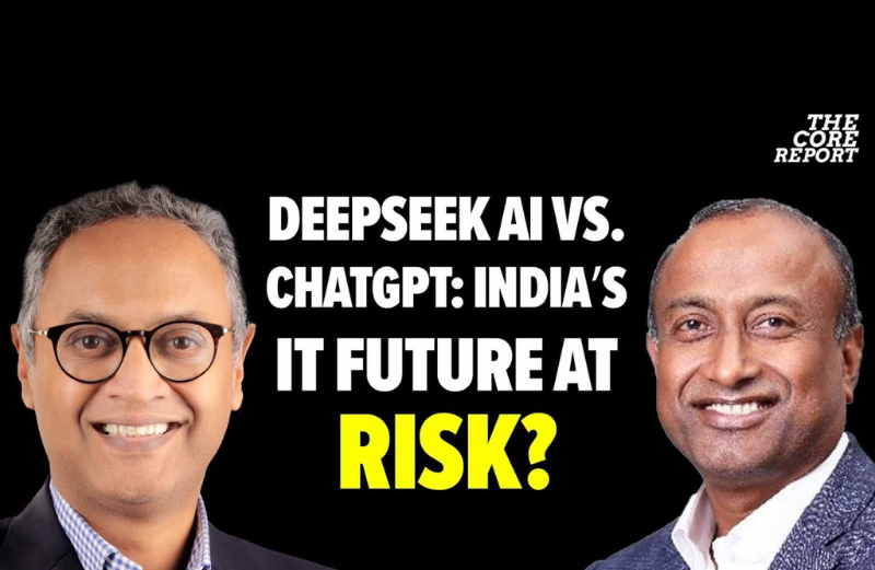
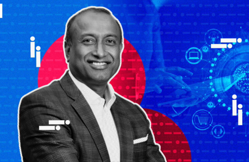
DeepSeek AI vs. ChatGPT: How India’s IT Sector Will Be Disrupted!
Nasscom President Rajesh Nambiar shared insights, while India’s finance ministry advised against using ChatGPT and DeepSeek over data security risks, similar to bans in Australia and Italy.

AI in Scientific Discovery & Ethics: Dr. Anima Anandkumar on the Future of AI
In this episode of nasscom Conversation, Dr. Anima Anandkumar, Bren Professor at Caltech, discusses the transformative role of AI in scientific discovery, ethical AI development, and AI-driven innovation.
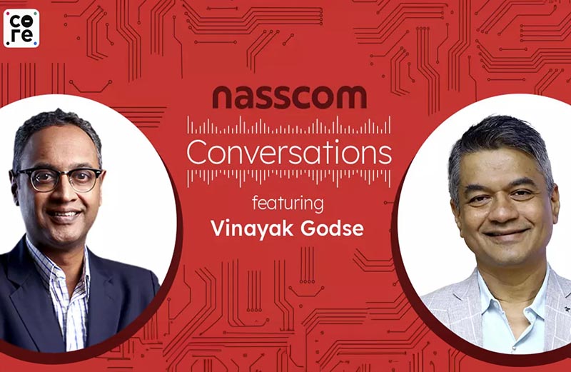
Cybersecurity Strategies for India with Vinayak Godse, CEO DSCI
In this episode of nasscom conversation, Vinayak Godse, CEO of the Data Security Council of India (DSCI), joins Govindraj Ethiraj to discuss the critical role of cybersecurity in India's digital economy.
Scaling and Nurturing AI Startups: Essentials for Success
Join Sangeeta Gupta, Senior Vice President & Chief Strategy Officer, nasscom alongside Matthias Zwingli, CEO and Founder of Connect AI, as they explore the dynamics of scaling AI startups.

Exploring India's AI and Tech Strategy Amid Global Geopolitics
In this episode, Dr. Venkat Raman discusses India's potential in the global AI race, China's impact on global supply chains, and the strategic role of IoT in geopolitics. The conversation explores how India can enhance its tech initiatives and what the evolving US-China dynamics could mean for Indo-US relations and tech investments in India.